Detecting a manufacturing defect is one decision. Choosing the right response is another
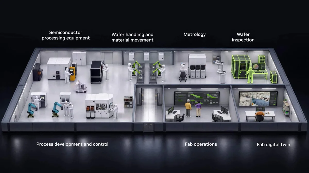
NVIDIA’s November 3 article on semiconductor fabs describes how accelerated simulation, physics-based AI, and digital twins help engineers explore process changes before physical trials. It connects with my research on deep learning for defect detection in additive manufacturing.
A vision model can identify a suspicious pattern in an image. Turning that prediction into useful process feedback requires more context: what was happening during production, which settings were active, and whether the observation points to a repeatable problem. I would structure that investigation around three questions: What did the model observe? Which process conditions could explain it? What experiment would distinguish between those explanations? For example, a suspected printing defect could prompt a review of images alongside process settings and timestamps, followed by a controlled test of one proposed cause. That keeps the model’s prediction connected to an engineering question that can be investigated. The opportunity I see is a tighter feedback loop between observation, analysis, and experimentation. When evaluating manufacturing AI, define the next decision its output should support—and the evidence needed to make that decision responsibly.
#ComputerVision #AdditiveManufacturing #AppliedAI